
Taidacent, широтно-импульсная модуляция, регулируемый ШИМ-контроллер скорости тока A4950, щеточный двигатель постоянного тока, DMOS, двойной полный мостовой драйвер
- Категория товара: Motor Drivers >>>
- Поставщик (Оптовый магазин): Shenzhen,Taida,Century,Technology,Co.,Ltd.
Поделиться:
Описание и отзывы
Характеристики
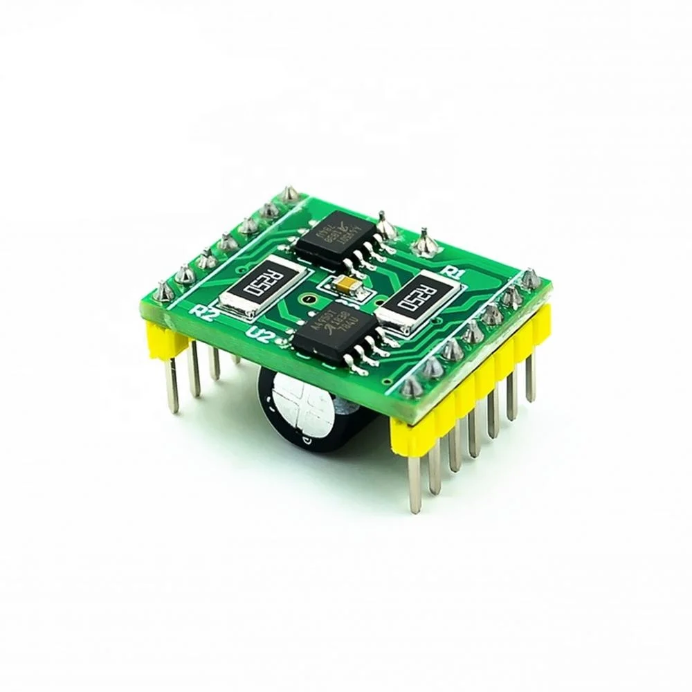
Taidacent Pulse Width Modulated Adjustable PWM Current Speed Controller A4950 DC Brushed Motor DMOS Dual Full Bridge Driver
Module parameters:
Function: It can control the positive and negative rotation of 2 motors (such as balancing the car, only one module is needed)
Voltage: 7.6~40V
Current: Module with current limit protection, 2A (overcurrent will not be powered off, only limit the maximum output current)
Control: 4 PWM pins are required. (If you do not need to reverse, only 2 PWM pins are needed.) It is much simpler to use than the L298 and provides instructions for use.
Weight: 3g
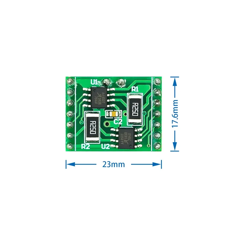
Size: 23*18.3mm
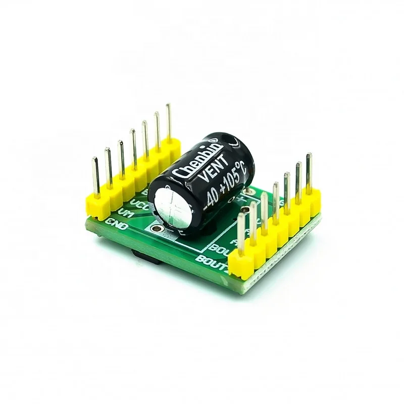
Lead 2 rows of 7Pin pin headers with a pitch of 20mm
| Size | 23*18.3mm |
| Voltage | 7.6~40V |
| Current | 2A |
Features and Benefits
Low RDS(on) outputs
Overcurrent protection (OCP)
Motor short protection
Motor lead short to ground protection
Motor lead short to battery protection
Low Power Standby mode
Adjustable PWM current limit
Synchronous rectification
Internal undervoltage lockout (UVLO)
Crossover-current protection
A4950K is AEC-Q100 Grade 1 qualified
Commercial temperature grade (A4950E: –40°C to 85°C)
Automotive temperature grade (A4950K: –40°C to 125°C)
Description
Designed for pulse width modulated (PWM) control of DC motors, the A4950 is capable of peak output currents to ±3.5 A and operating voltages to 40 V. Input terminals are provided for use in controlling the speed and direction of a DC motor with externally applied PWM control signals. Internal synchronous rectification control circuitry is provided to lower power dissipation during PWM operation. Internal circuit protection includes overcurrent protection, motor lead short to ground or supply, thermal shutdown with hysteresis, undervoltage monitoring of VBB, and crossovercurrent protection. For high ambient operating temperature applications, an automotive grade device is offered (A4950K). The K grade device is tested across extended temperature and voltage ranges to ensure compliance in automotive or industrial applications. The A4950 is provided in a low-profile 8-pin SOICN package with exposed thermal pad (suffix LJ) that is lead (Pb) free, with 100% matte tin leadframe plating.
Functional Description
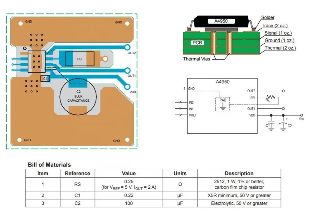
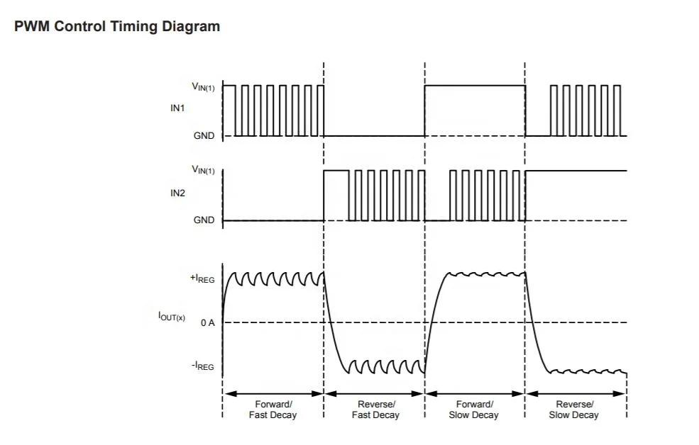
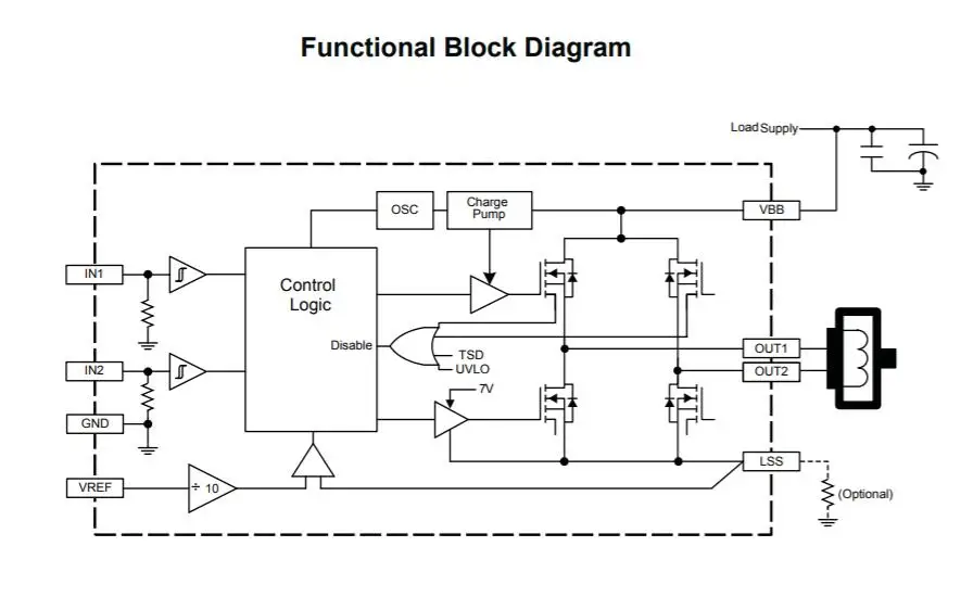
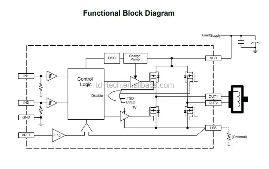
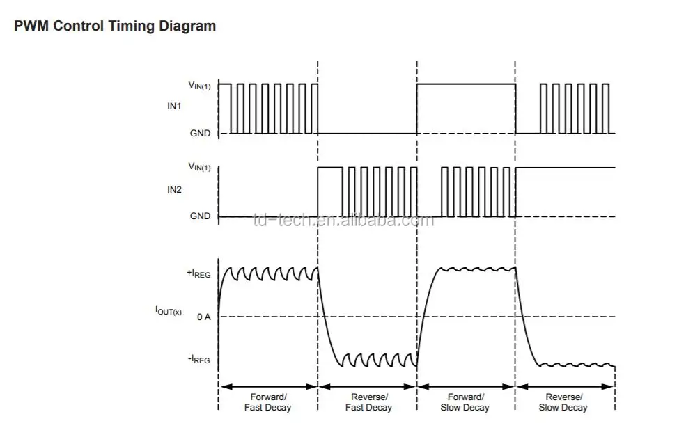
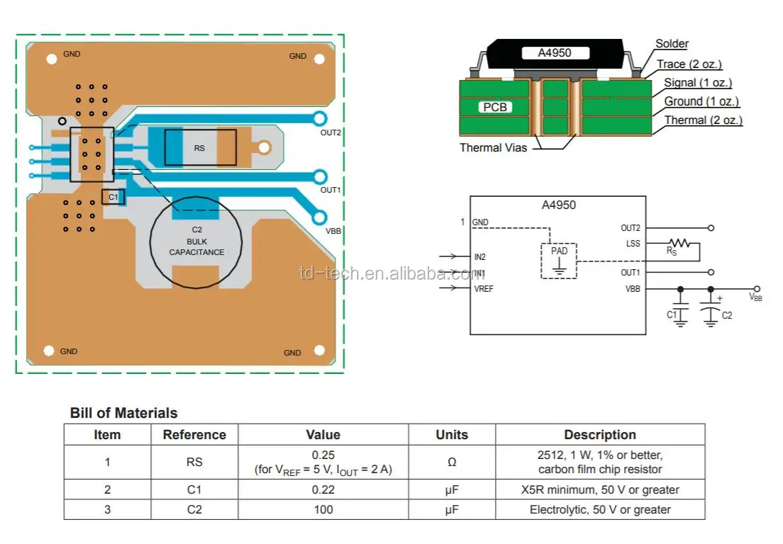
The A4950 is designed to operate DC motors. The output drivers are all low-RDS(on) , N-channel DMOS drivers that feature internal synchronous rectification to reduce power dissipation. The current in the output full bridge is regulated with fixed off-time pulse width modulated (PWM) control circuitry. The IN1 and IN2 inputs allow two-wire control for the bridge. Protection circuitry includes internal thermal shutdown, and protection against shorted loads, or against output shorts to ground or supply. Undervoltage lockout prevents damage by keeping the outputs off until the driver has enough voltage to operate normally. Standby Mode Low Power Standby mode is activated when both input (INx) pins are low for longer than 1 ms. Low Power Standby mode disables most of the internal circuitry, including the charge pump and the regulator. When the A4950 is coming out of standby mode, the charge pump should be allowed to reach its regulated voltage (a maximum delay of 200 μs) before any PWM commands are issued to the device. Internal PWM Current Control Initially, a diagonal pair of source and sink FET outputs are enabled and current flows through the motor winding and the optional external current sense resistor, RS . When the voltage across RS equals the comparator trip value, then the current sense comparator resets the PWM latch. The latch then turns off the sink and source FETs (Mixed Decay mode). VREF The maximum value of current limiting is set by the selection of RSx and the voltage at the VREF pin. The transconductance function is approximated by the maximum value of current limiting,
ITripMAX (A), which is set by: ITripMAX = 10 RS VREF where VREF is the input voltage on the VREF pin (V) and RS is the resistance of the sense resistor (Ω) on the LSS terminal. Overcurrent Protection A current monitor will protect the IC from damage due to output shorts. If a short is detected, the IC will latch the fault and disable the outputs. The fault latch can only be cleared by coming out of Low Power Standby mode or by cycling the power to VBB. During OCP events, Absolute Maximum Ratings may be exceeded for a short period of time before the device latches. Shutdown If the die temperature increases to approximately 160°C, the full bridge outputs will be disabled until the internal temperature falls below a hysteresis, TTSDhys , of 15°C. Internal UVLO is present on VBB to prevent the output drivers from turning-on below the UVLO threshold. Braking The braking function is implemented by driving the device in Slow Decay mode, which is done by applying a logic high to both inputs, after a bridge-enable Chop command (see PWM Control Truth Table). Because it is possible to drive current in both directions through the DMOS switches, this configuration effectively shorts-out the motor-generated BEMF, as long as the Chop command is asserted. The maximum current can be approximated by VBEMF / RL . Care should be taken to ensure that the maximum ratings of the device are not exceeded in worse case braking situations: high speed and high-inertia loads.
Похожие товары


Сервопривод и Сервопривод переменного тока
US $230.00-$550.00


Новый Серводвигатель HFC 750 Вт
US $289.20
