
TEC1-12712 12V 12A 40*40MM Heatsink Thermoelectric Cooler Cooling Peltier Plate Module
- Category: Semiconductors >>>
- Seller: Changzhou,Boyan,Optical,Co.,Ltd.
Share on:
Product Overview
Description
Product Description
Specification
item | value |
Place of Origin | China |
Jiangsu | |
Brand Name | BOYAN |
Model Number | SiO2 |
Type | Quartz Wafer |
Materia | Synthetic Quartz Crystal |
Cutting Angle | X/Y/Z/AT32°/33°/35°/36°/BT/ST42.75°-cut etc per Customized |
Diameter/size | 3" 4" 6" 8" |
Tol(±) for Diameter | <0.20 mm |
LTV (5mmx5mm) | <1.5μm |
TTV | <1.5~3 μm |
Bow | -30 |
Warp | <40μm |
PLTV(<0.5um) | ≥95%(5mm*5mm) |
Orientation Flat | All available |
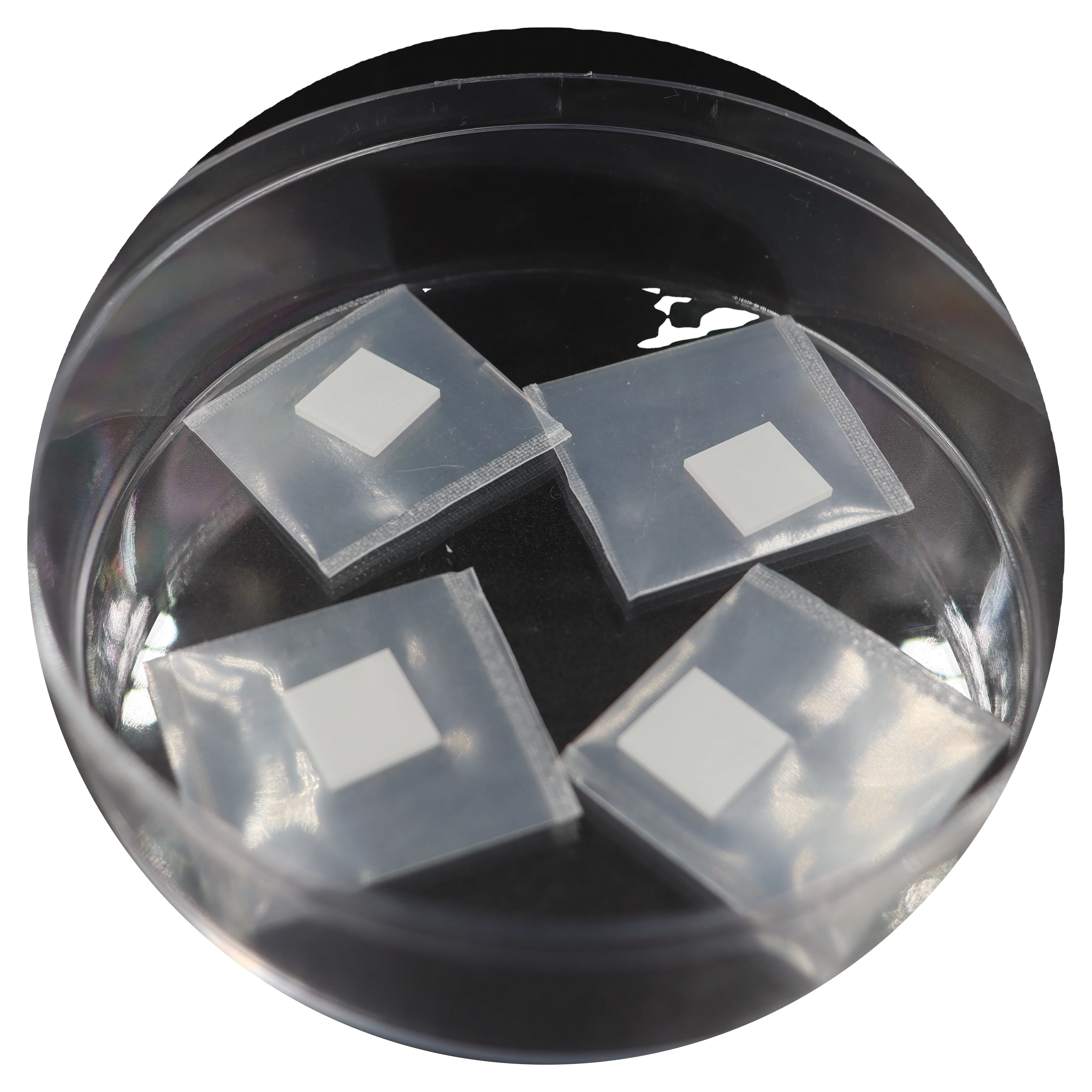
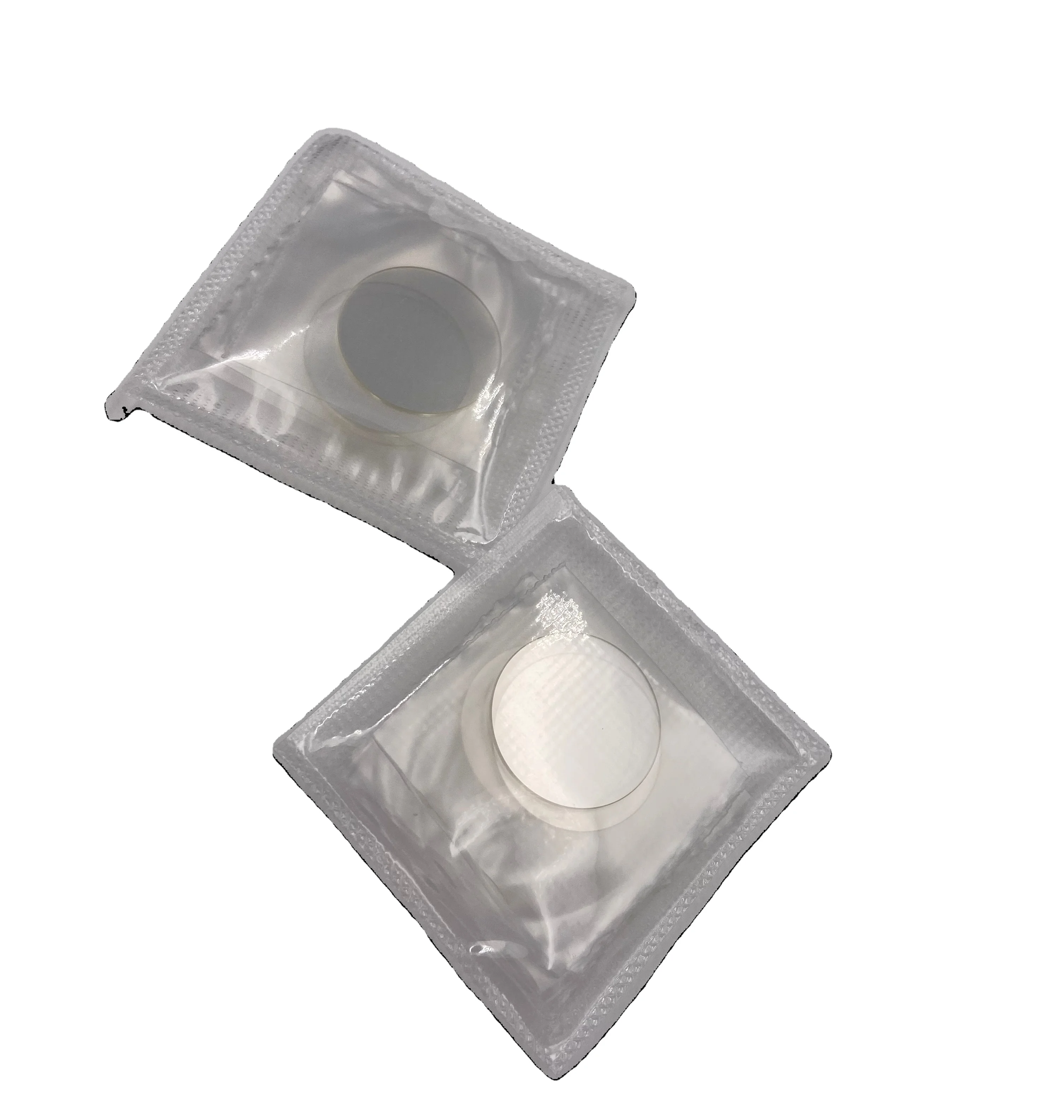
Packing & Delivery
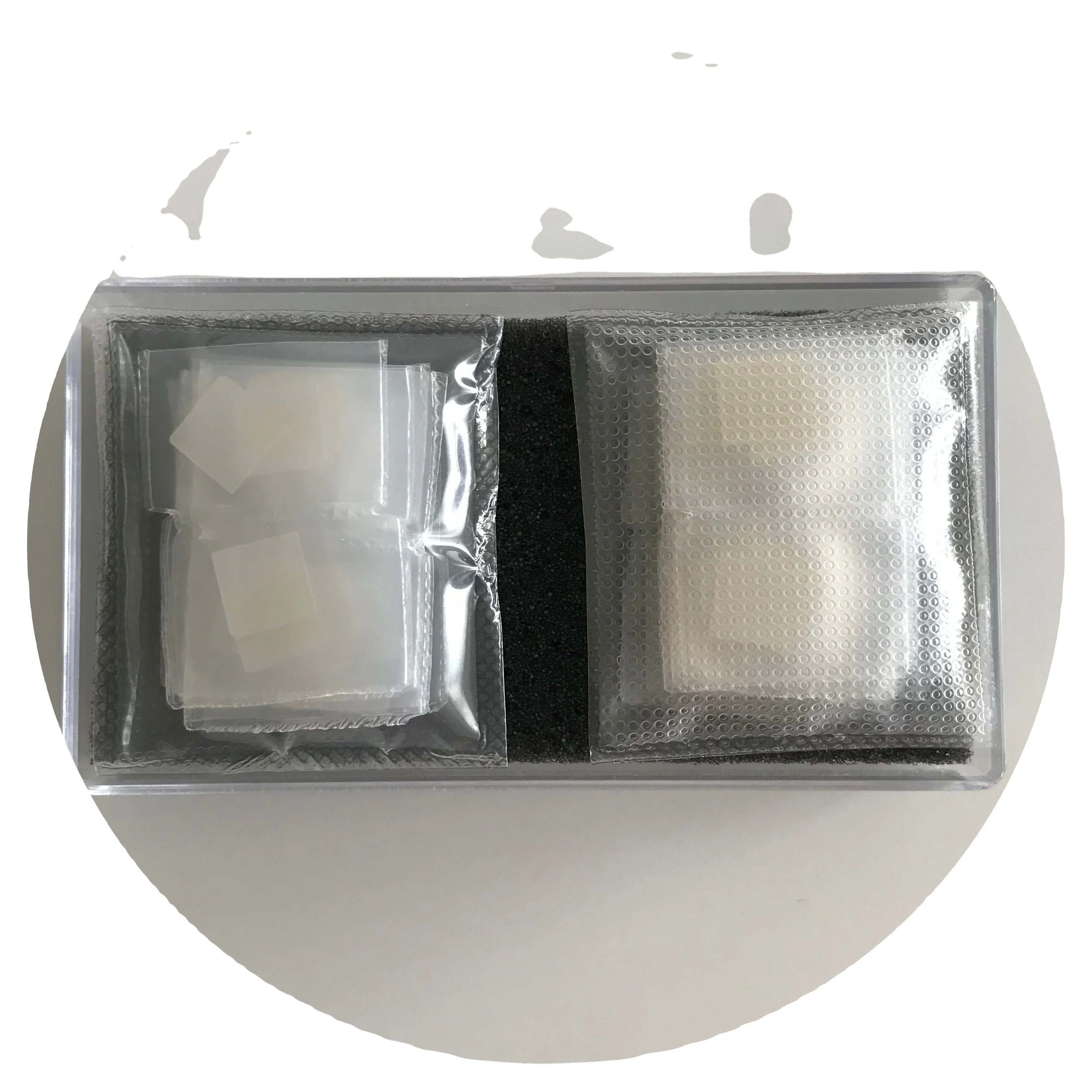
For cutting pieces
For small cutting ,we will do 100 degree ultra-clean polybag package
For 2 " or large size small quantity
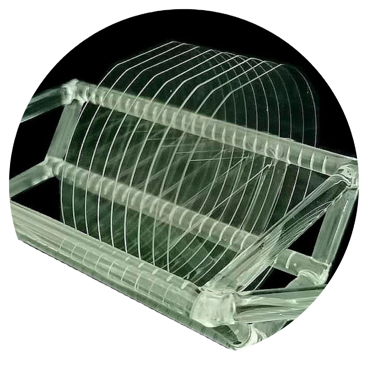
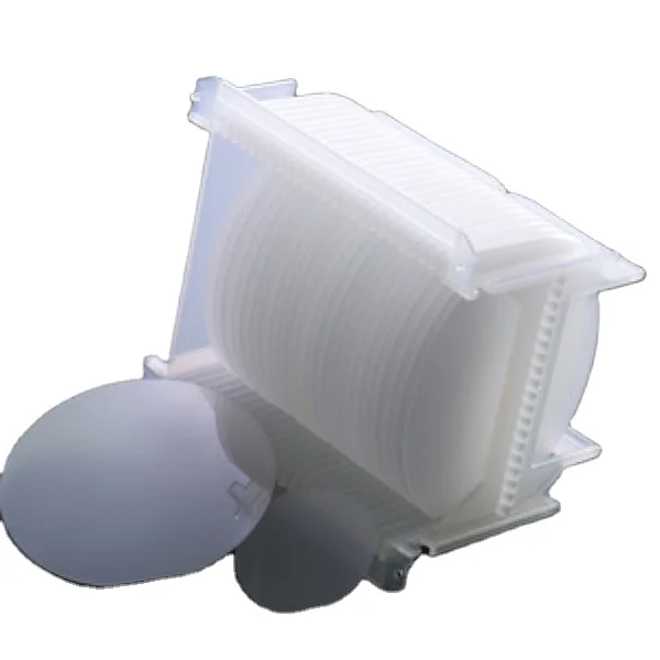
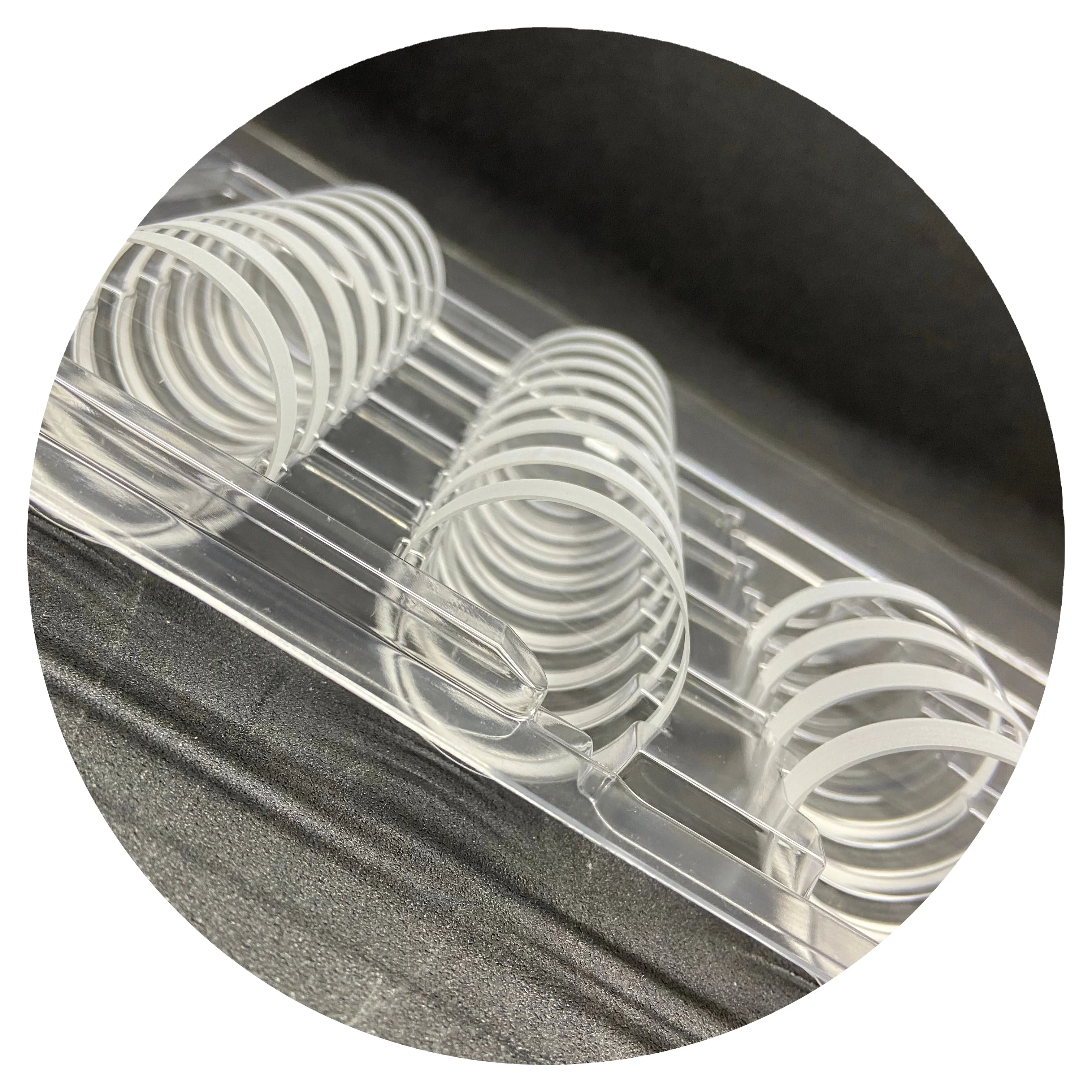
For size 2 /3/4/6/8 inches wafers ,with small quantity ,we will use single wafer carrier to handle to package
For Bulk shipping
For quantity with 25 pcs ,we will use bulk order package
Company Profile

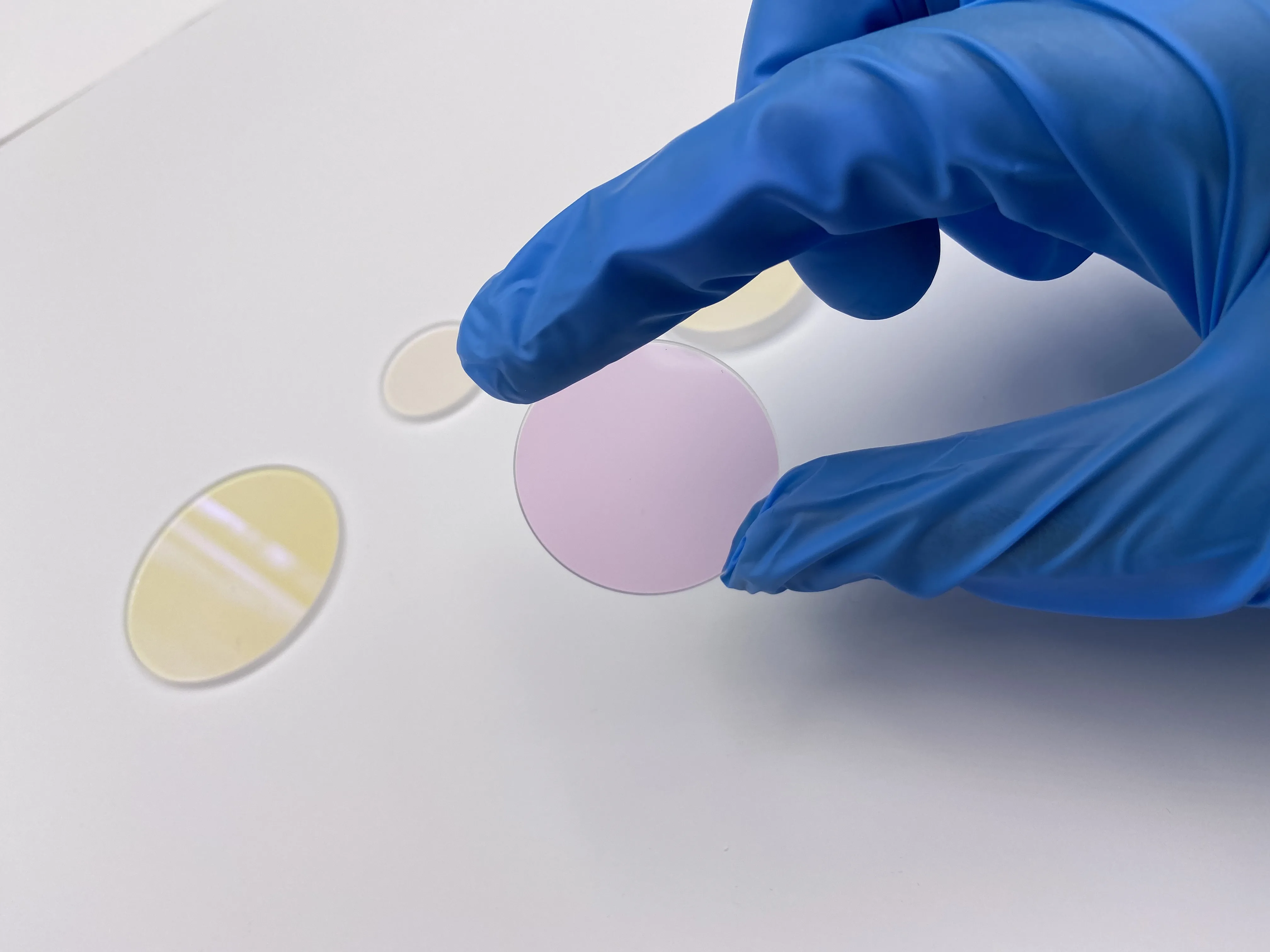
Changzhou Boyan Optical Co., Ltd. is a multi-product high-tech company specializing in the research, development, production and sales of flat windows, crystals ,optical components ,wafers & substrates and coated glassed.
The company mainly provides colored glass, colorless glass, infrared filters, ultraviolet filters, far-infrared crystals, lenses, prisms, cylindrical lens, sapphire wafers, silicon wafers and various coating products The application band of product materials ranges from ultraviolet to mid-far infrared such as: fused quartz, sapphire, magnesium fluoride, lithium fluoride, barium fluoride, silicon, germanium, zinc selenide, zinc sulfide and various colored and colorless optical materials .


What we can offer
New Crystal | ||||||||
Cu2O | Fe2O3 | SnO2 | Fe2O3 | MnO | ||||
ZnO/Al2O3 | ||||||||
Superconducting thin film | ||||||||
SrTiO3 | YSZ | MgO | KTaO3 | |||||
Functional epitaxial thin films | ||||||||
SiO2 + Si | GaN on Sapphire wafer | Pt/Ti/SiO2/Si wafer | ||||||
Photo Transistor substrate | ||||||||
GGG substrate | Nb:SrTiO3 substrate | Fe:SrTiO3 substrate | PMN-PT substrate | |||||
Photo Transistor substrate | ||||||||
TiO2 Rutile substrate | SiO2 quartz monocrystal substrate | YAlO3 substrate | ||||||
quartz glass substrate | YAG substrate | LiNbO3 substrate | LiTaO3 substrate | |||||
Semiconducting crystal substrate | ||||||||
InSb substrate | Si substrate | InP substrate | InAs substrate | |||||
Fluo-chloride crystal substrate | ||||||||
MgF2 substrate | CaF2 substrate | BaF2 substrate | LiF substrate | KCl substrate | ||||
NaCl substrate | KBr substrate | |||||||
III-V crystal substrate | ||||||||
Sapphire wafer | GaN monocrystal substrate | LiAlO2 substrate | MgAl2O4 substrate | |||||
II-VI crystal substrate | ||||||||
ZnO high resistivity substrate | ZnO low resistivity substrate | Ga:ZnO substrate | ||||||
Ceramic substrate | ||||||||
Al2O3 96% substrate | AlN ceramic substrate | YSZ ceramic | ||||||
Other materials | ||||||||
Cu metal monocrystal substrate | Al metal monocrystal substrate | KTa(1-x)Nb(x)O3 | ||||||
Mg metal monocrystal substrate | K9 glass substrate | Sapphire Tube | Ruby Tube | |||||
FTO Glass | ITO glass | |||||||
FAQ
Q: What is the shipping option ?
A: We have Fedex and DHL ,SF international shipping for small orders , for bulk orders over 100 kgs ,we prefer air shipping to local airport
Q: How long is your delivery time?
A: Generally it is 3~7 days if the goods are in stock. or it is 15-20 days if the goods are not in stock, it is according to
quantity.
Q: Do you provide samples ? is it free or extra ?
A: Yes, we could offer the sample ,but we need to take the sample fee .
Q: What is your terms of payment ?
A: Payment<=1000USD, 100% in advance. Payment>=1000USD, 30% T/T in advance ,balance before shippment.
A: We have Fedex and DHL ,SF international shipping for small orders , for bulk orders over 100 kgs ,we prefer air shipping to local airport
Q: How long is your delivery time?
A: Generally it is 3~7 days if the goods are in stock. or it is 15-20 days if the goods are not in stock, it is according to
quantity.
Q: Do you provide samples ? is it free or extra ?
A: Yes, we could offer the sample ,but we need to take the sample fee .
Q: What is your terms of payment ?
A: Payment<=1000USD, 100% in advance. Payment>=1000USD, 30% T/T in advance ,balance before shippment.


